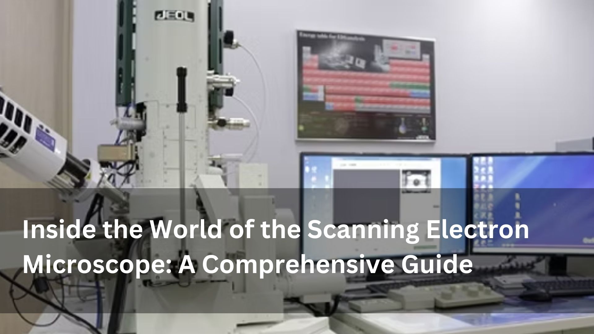
In the ever-evolving field of microscopy, the scanning electron microscope (SEM) stands out as a powerful and essential tool for scientists and engineers alike. Unlike traditional optical microscopes, the scanning electron microscope uses electrons instead of light to form highly detailed images of a specimen’s surface. This breakthrough in imaging allows researchers to observe materials at the micro and nano scales, offering unparalleled resolution and depth of field. Whether you’re studying biological specimens, inspecting semiconductor devices, or analyzing forensic samples, the scanning electron microscope provides the clarity and precision needed for accurate interpretation and innovation.
What is a Scanning Electron Microscope?
A scanning electron microscope (SEM) is a powerful imaging instrument that uses a focused beam of electrons to generate highly detailed surface images of materials. Unlike traditional optical microscopes, SEMs offer incredibly high magnification (up to 2 million times) and superior depth of field, revealing the intricate topography and composition of samples.
How Does a Scanning Electron Microscope Work?
The working principle of a scanning electron microscope involves scanning a sample with a focused beam of electrons. When these electrons interact with the atoms of the specimen, they produce secondary electrons, backscattered electrons, and characteristic X-rays. These signals are then detected and translated into an image or chemical data.
Key components include:
Electron Gun: Emits a beam of electrons.
Electromagnetic Lenses: Focus the electron beam.
Detectors: Capture secondary and backscattered electrons.
Vacuum Chamber: Prevents electron scattering by air molecules.
Types of Scanning Electron Microscopes
There are several types of scanning electron microscopes, each tailored to different applications:
Conventional SEM: General-purpose, high-resolution imaging.
Environmental SEM (ESEM): Allows imaging in humid or gas environments.
Field Emission SEM (FE-SEM): Offers improved resolution for nanoscale imaging.
Advantages of Using a Scanning Electron Microscope
Utilizing a scanning electron microscope offers several advantages:
High Magnification & Resolution: Observe minute details invisible to light microscopes.
3D Surface Imaging: Reveals texture, cracks, and morphological features.
Elemental Analysis: Paired with Energy-Dispersive X-ray Spectroscopy (EDS).
Wide Range of Materials: Works on metals, polymers, ceramics, and biological specimens.
Applications of Scanning Electron Microscopes in Research
In academic and industrial research, the scanning electron microscope plays a vital role:
Material Science: Analyzing grain structures, fractures, and coatings.
Biology & Medicine: Visualizing cells, viruses, and tissue structures.
Nanotechnology: Inspecting nanomaterials, nanotubes, and quantum dots.
Semiconductors: Investigating microchips and integrated circuits.
Industrial Uses of Scanning Electron Microscopes
Beyond laboratories, the scanning electron microscope is critical in quality control and failure analysis:
Automotive: Studying wear and fatigue in engine parts.
Aerospace: Inspecting turbine blades and composite materials.
Forensics: Analyzing gunshot residues, paint chips, and tool marks.
Pharmaceuticals: Ensuring uniformity and purity in drug particles.
Sample Preparation for SEM Analysis
Proper sample preparation is crucial for accurate scanning electron microscope results:
Drying: Samples must be free from moisture.
Mounting: Attached to a stub with conductive adhesive.
Coating: Non-conductive samples often need a thin metal (gold/palladium) coating.
Sectioning: Cross-sectioning helps study internal structures.
Limitations and Challenges of Scanning Electron Microscopes
Despite their power, scanning electron microscopes have limitations:
Cost: High initial and operational expense.
Sample Constraints: Requires vacuum compatibility and electrical conductivity.
Training: Skilled operators are necessary.
Size: Large equipment footprint.
The Future of Scanning Electron Microscopy
The scanning electron microscope continues to evolve with exciting advancements:
Automated Analysis: AI-driven feature recognition and defect mapping.
Compact Designs: Desktop SEMs for easier integration in labs.
Cryo-SEM: Allows imaging of hydrated biological samples in frozen state.
Hybrid Systems: Integrating SEM with other imaging tools like AFM and TEM.
Conclusion
The scanning electron microscope is a cornerstone of modern scientific exploration and industrial precision. Its ability to reveal ultra-fine details of surface structures and compositions has transformed research, development, and quality control across countless fields. As technology advances, SEMs will become even more powerful, accessible, and essential, opening new frontiers in science and innovation.
Whether you’re analyzing microchips, studying cells, or developing new materials, the scanning electron microscope offers unmatched clarity and depth, ensuring a deeper understanding of the microscopic world around us.


