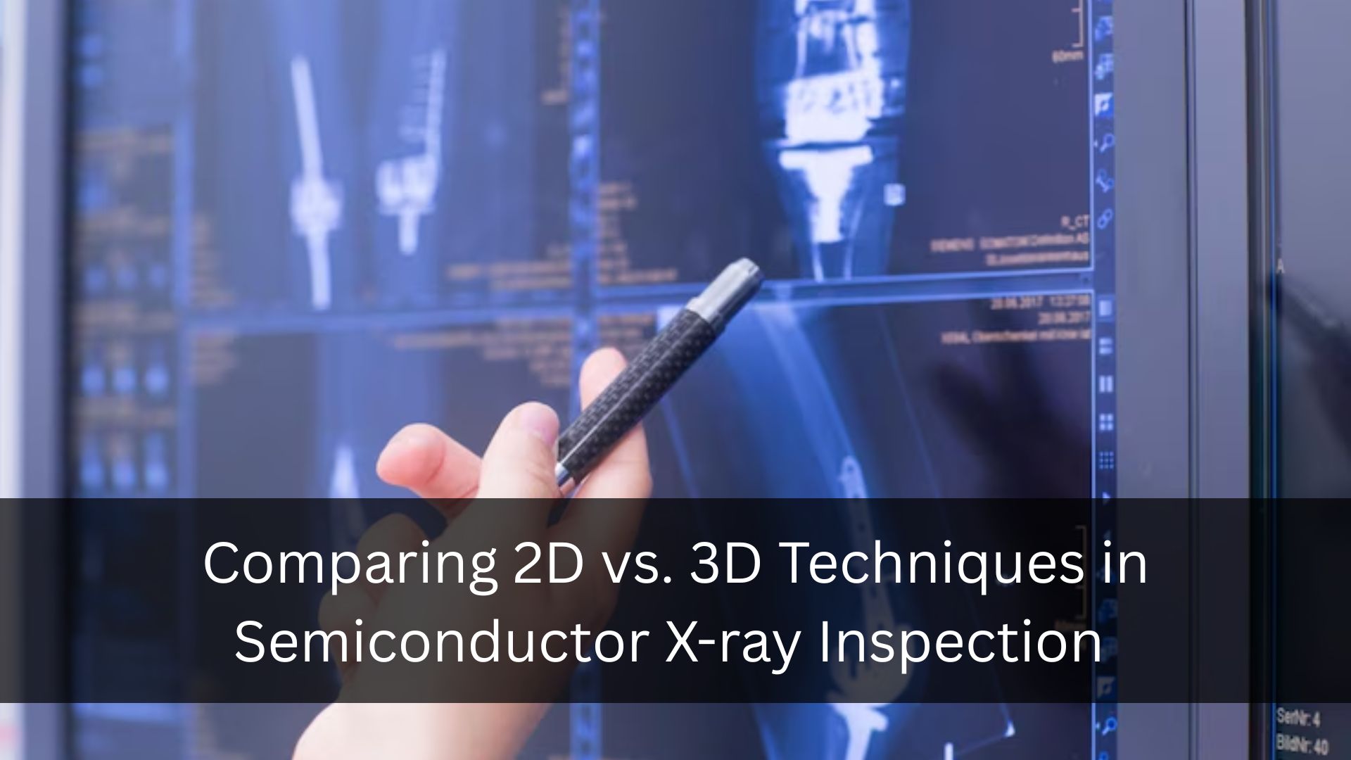
Understanding Semiconductor X-ray Inspection Techniques
Semiconductor X-ray inspection is a non-destructive testing method that uses X-ray radiation to visualize the internal features of semiconductor devices. This allows manufacturers to inspect solder joints, die bonds, wire connections, and package alignment without damaging the components. The primary goal is to detect defects that are not visible externally, such as voids, cracks, delamination, or misplaced interconnects.
Depending on the inspection depth and dimensional accuracy required, manufacturers choose between two main types of X-ray imaging:
- 2D X-ray inspection: Produces flat, grayscale images representing a projection of the internal structure.
- 3D X-ray inspection (also known as X-ray computed tomography or CT): Generates volumetric reconstructions that reveal detailed internal geometry in three dimensions.
Each method has its strengths and limitations, which we will explore below.
Key Differences Between 2D and 3D Semiconductor X-ray Inspection
1. Imaging Process and Output
2D Semiconductor X-ray Inspection
In 2D inspection, a single or limited-angle X-ray source projects radiation through the semiconductor component onto a detector. The result is a flat image that overlays all internal structures. This projection allows quick identification of anomalies but lacks depth information.
3D Semiconductor X-ray Inspection
3D inspection uses a rotating sample or a moving X-ray source to capture multiple images from different angles. These images are compiled using reconstruction algorithms to create a volumetric model. This enables inspectors to slice through the object layer-by-layer, examining specific depths and dimensions.
2. Accuracy and Detail
2D imaging is suitable for detecting general defects such as voids, missing connections, or major alignment issues. However, because everything is overlaid in a single plane, subtle defects hidden beneath larger features can be missed.
3D imaging, on the other hand, provides unmatched clarity and detail. It allows users to zoom in on specific layers and structures, isolate defects in three dimensions, and measure distances, volumes, and shapes with high precision. This makes 3D ideal for complex packaging, such as system-in-package (SiP), 3D ICs, and BGA assemblies.
3. Inspection Speed
2D X-ray inspection is much faster than 3D. Because it captures fewer images and requires less data processing, it is well-suited for high-throughput environments like production lines or incoming inspection. It allows for real-time feedback and continuous monitoring without significant delay.
3D X-ray inspection requires more time for data acquisition and image reconstruction. This makes it more suitable for sample testing, failure analysis, and applications where inspection depth outweighs speed. However, advances in computing and automation are helping to close the gap between 2D and 3D inspection times.
4. Equipment Complexity and Cost
2D systems are generally simpler, more compact, and less expensive. They require fewer moving parts and consume less power, making them an attractive option for small to mid-sized operations or where space is limited.
3D systems involve advanced hardware, rotating stages, higher-resolution detectors, and more powerful software. These features increase both the cost and complexity of the equipment. However, for high-reliability sectors like aerospace, medical electronics, or automotive safety systems, the return on investment is significant.
Advantages of 2D Semiconductor X-ray Inspection
- Speed and Efficiency: Ideal for large-scale production lines and quick defect screening.
- Lower Cost: Equipment and maintenance costs are lower, making it more accessible.
- Simplicity: Easier to operate and requires less training.
- Good for Basic Defects: Sufficient for detecting large voids, missing components, or alignment issues.
Advantages of 3D Semiconductor X-ray Inspection
- High Precision: Excellent for detecting small or deeply embedded defects.
- Volumetric Analysis: Allows for detailed measurements and dimensional checks.
- Layer-by-Layer Evaluation: Enables inspection of individual package layers and bond interfaces.
- High Precision: Excellent for detecting small or deeply embedded defects.
- Better Failure Analysis: Essential for root cause analysis in product recalls or critical failures.
When to Use 2D vs. 3D in Semiconductor X-ray Inspection
Use 2D Inspection When:
- You require high-speed inspection of large volumes.
- The components are relatively simple or defects are usually near the surface.
- You are performing routine quality control on known-good designs.
- You require high-speed inspection of large volumes.
- Cost and space limitations are a major consideration.
Use 3D Inspection When:
- Your products involve complex geometries or multilayer structures.
- Defects are known to occur deep within packages.
- You need precise measurements for research, development, or failure analysis.
- Your products involve complex geometries or multilayer structures.
- Meeting strict industry standards or certifications is critical.
Practical Applications in the Semiconductor Industry
In real-world semiconductor manufacturing, both 2D and 3D X-ray inspection techniques are often used in combination. For example:
- Incoming material inspection might use 2D imaging for fast verification of lead frames, substrates, or wafers.
- In-line inspection of PCBs or BGAs can begin with 2D and escalate to 3D for units that trigger anomaly flags.
- Failure analysis labs use 3D imaging extensively to dissect failed units and determine the exact location and nature of defects.
- R&D teams rely on 3D X-ray inspection to validate new package designs and refine bonding techniques.
Challenges and Future Developments
As electronics continue to evolve, inspection methods must adapt. Some challenges in semiconductor X-ray inspection include:
- Resolution limits in 2D systems for ultra-fine-pitch features.
- Data volume and processing time in 3D systems.
- Cost constraints that may limit access to advanced imaging in smaller facilities.
Looking ahead, integration with AI and machine learning promises to revolutionize both 2D and 3D X-ray inspection. Smart defect recognition, automated pass/fail grading, and predictive maintenance based on inspection trends are just a few innovations on the horizon.
Another exciting development is hybrid imaging, where 2D and 3D data are combined into a comprehensive inspection workflow. This offers the speed of 2D with the precision of 3D, creating a more balanced approach to semiconductor quality control.
Conclusion
Both 2D and 3D techniques in semiconductor X-ray inspection have distinct roles to play in the quest for quality and reliability. While 2D inspection offers speed, simplicity, and cost-efficiency, 3D inspection provides deeper insight, higher accuracy, and the ability to tackle complex assemblies.
The decision between the two methods depends on the specific needs of the manufacturing process, the complexity of the components, and the level of precision required. In many cases, the best approach involves using both techniques strategically to create a layered and adaptive inspection strategy.
As the industry continues to demand smaller, faster, and more powerful devices, semiconductor X-ray inspection—in both 2D and 3D forms—will remain a cornerstone of quality assurance and innovation in electronics manufacturing.