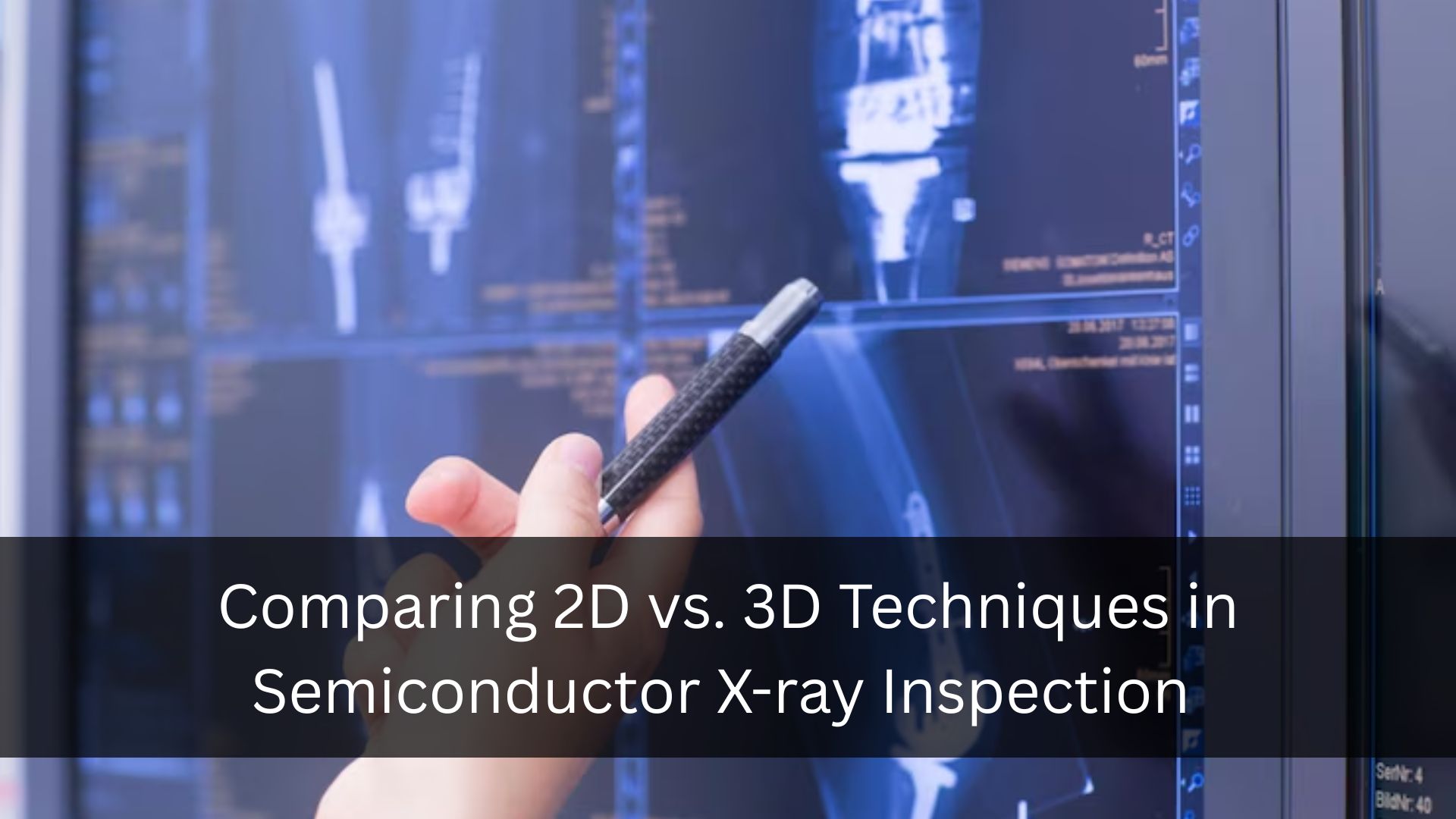
In the ever-evolving world of electronics manufacturing, the demand for miniaturization, high performance, and quality assurance is driving significant innovations in inspection technologies. Among these, semiconductor X-ray inspection has emerged as a critical method for detecting internal defects and verifying the structural integrity of components. As manufacturers seek more precise and reliable data, the debate between 2D and 3D X-ray techniques continues to gain attention. This article explores the core differences between 2D and 3D semiconductor X-ray inspection, the advantages of each method, and how to choose the right solution for your inspection needs.